Research highlight from our recent N. Stewart McIntyre award winner Matthew J. Turnbull, Department of Chemistry, Western University.
The primary goal of this research is to elucidate the key features that differentiate nanocrystal-based CZTS films from their crystalline counterparts.
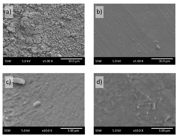
As indicated in Figure 1, there are three main mechanisms by which electrons move from the valence band in the absorber layer through the solution. This provides a measure of the number of electrons liberated from a film under illumination. Both nanocrystal-based and crystalline films of equivalent photoresponse have been fabricated, yet on transition to a solid-solid interface, the nanocrystals show significantly less output. From the SEM images (Fig. 2), the surface morphologies differed, making a much larger surface area over which the nanocrystalline CZTS formed a p-n junction.

Figure 1: Mechanistic electron flow from the absorber layer through solution. Light strikes the surface, generating an electron-hole pair. The electron is transferred to MV2+, where it can either recombine, or separate completely.

Figure 2: SEM images of a) CZTS NC, and b) crystalline CZTS films. The individual NC clusters can be seen in c), and are lacking in the crystalline d).
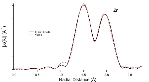
Using synchrotron-based extended X-ray absorption fine structure (EXAFS), the different CZTS surfaces were analyzed for composition. The Zn-sites of the crystalline films showed only Zn-S bonds as the nearest neighbour, as expected. The nanocrystal-based films, however, showed two peaks (Fig. 3), one to sulfur, and one to the oxygen atom of water. Removing the water removed the barrier to product separation, and resolved the discrepancies between the two CZTS films.

Figure 3: Zn EXAFS data fit for a two-atom first nearest neighbour for surface level Zn centers. The first peak results from Zn-OH2 bonds, while the second results from Zn-S bonds expected for CZTS.

